DeltaLab DL-4 Rack Delay Unit
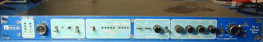
I recently purchased a non-working DL-4, to learn about how it worked and see if I could get it going. I had heard that this was a good-sounding unit, and knew that it used a different way of encoding the audio signal digitally.
The unit did power on, but no delayed audio was present. I checked the four power supply voltage regulators, and found that one was getting hot and putting out close to 0 volts. I unplugged the power supply from the rest of the unit, but the problem persisted. Then I noticed several tantalum capacitors on the power supply board. One of these was shorted, so I replaced it and the "bad" regulator began putting out 15V. I thought this was going to be an easy repair. Guess again! There was still no delayed audio signal. I could see that the top pcb held the analog circuits, and the bottom one was for the digital delay. The only schematics I could find were for the DL-2, which is rather different, and the Effectron Jr, which is closer, but not close enough to be very useful. I could buy the schematic for the DL-4, but the price was almost what I paid for the DL-4, and seemed a ridiculous amount to pay for a schematic diagram. I found what seemed to be the digital data feeding from the top board down to the digital pcb. This signal changed when the input audio changed. There are 8 4116 16Kx1 DRAM's which would be the delay memory. I could see that the data inputs to these chips were always low, which explains why there was no delayed audio output. I found that the digitized audio after it enters the lower pcb, is then fed to the Ext/Int switch on the back panel, and then back to the digital pcb. The switch was not passing the signal. I cleaned the contacts and got the signal to appear back on the pcb. Still no joy. This is when I decided that I would need to draw out the schematic for the digital pcb. (You can find it below) Having the schematic made a huge difference, of course, and drawing it helped me to get familiar with the circuit and start to understand its function. I discovered that one of the 4116 DRAMs had failed. Luckily, I have some of these and was able to replace it easily. At this point I started to get delayed audio from the unit, but only using certain delay settings. Settings 2, 8, and 32 seemed to be working. I was feeding in a 1 KHz sine wave tone, so simply delaying it did not change the sound. I decided to see which DRAMs were being used in these modes, and found that only one bank of four DRAMs was needed. In fact, the 2 setting used just one of the 8 DRAMs. So one bank of DRAMs was working OK. This let me focus on signals that were used by the other bank of four DRAMs, and I found a 4011 (U3 in my schems) that was not working. I replaced this chip and now all delay settings were working.
No connectors!
The DL-4 circuitry is placed on five pc boards. Power supply, front controls, rear jacks, top analog circuits and bottom digital delay circuits. With one exception, these boards are hard-wired to each other with cables soldered at both ends. The bottom pcb cannot be removed from the underside of the unit. It's mounted under the top board on a metal frame that must be removed from the top of the unit. As far as I can tell, to replace a logic chip on the bottom board, you need to unsolder 60 wires. This is four 10-conductor cables, and one 20-conductor one. At first I thought that I must be mistaken about this. After unsoldering these 60 wires, I decided that I was not going to solder them back. With the boards removed for repair, there is no way to test them, so you would need to re-solder all 60 wires, test, then unsolder them again if a second bad chip had to be replaced on the digital pcb. This was not acceptable to me. I was determined to add connectors for all of these wires. Here are the results:
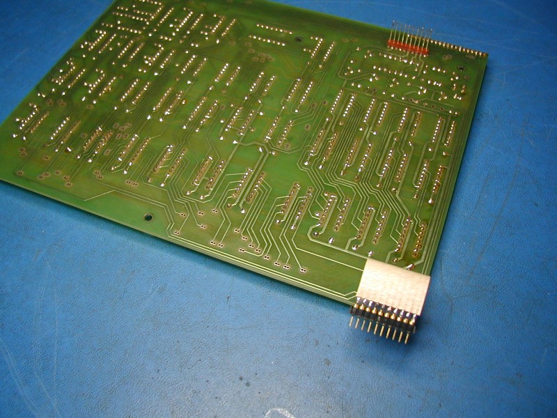
Digital board with cable modified:
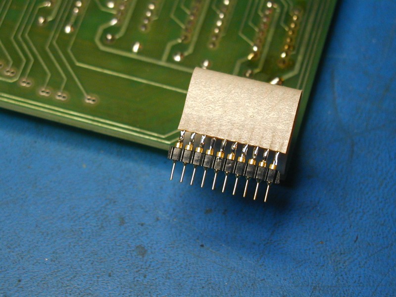
Close-up of Digital board cable modification:
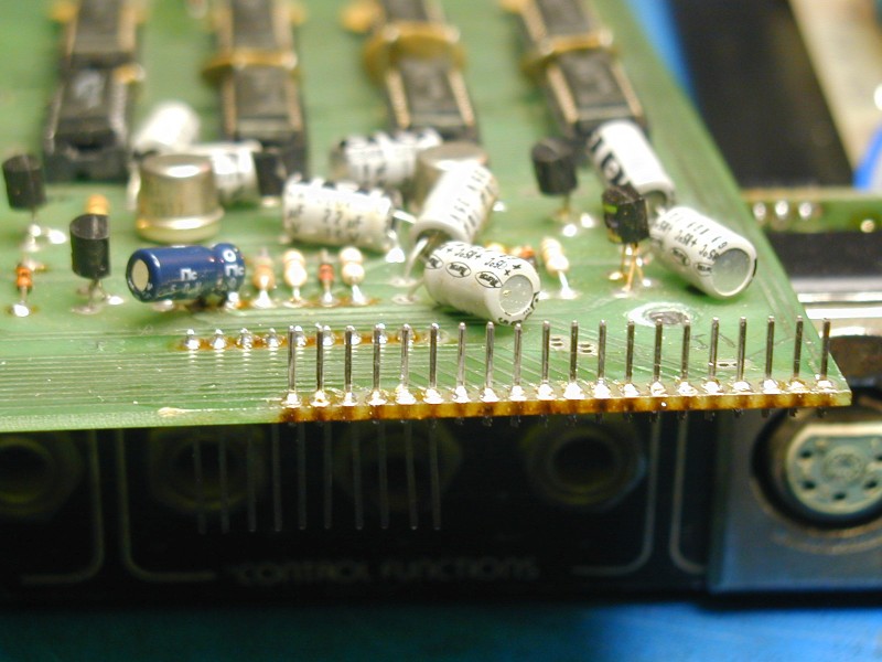
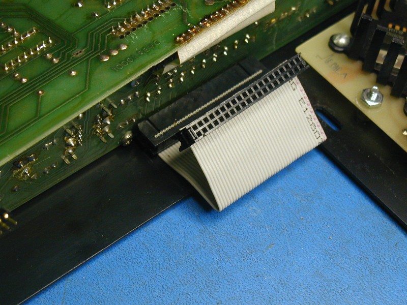
Digital board new header pins for ribbon cable connection to front panel: (No room for plastic part of header, just the pins)
Cable connecting front panel to digital board. Front panel board has same header pins as shown above. Note: Some 40-pin IDC females are smaller than others and must be used.
At front panel end, lower row of holes is used. At digital pcb end, holes closer to the end of the cable are used. This mod was the trickiest, as space is very tight.
Cables on the top side with connector mods. Large cable from analog pcb to front panel is left alone. Analog pcb can be folded up and over with this cable in place.
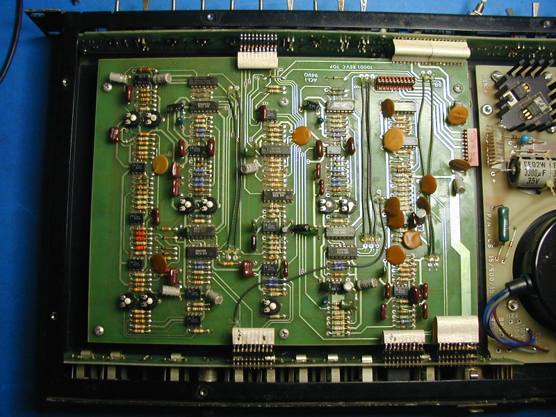
With these connectors installed, the bottom pcb can be removed for servicing without using a soldering iron.
My schematic for the DL-4 digital PCB:
Here it is. I did not capture schematics for the other pc boards.
Please note: Taking a DL4 apart and installing these mods must be done carefully, or damage to the unit will result. It should only be attempted by someone familiar with this type of work. I will not be responsible for any damage to any unit caused by either proper or improper use of the information presented here.