Sencore LC77/LC102 Capacitor - Inductor Analyzer
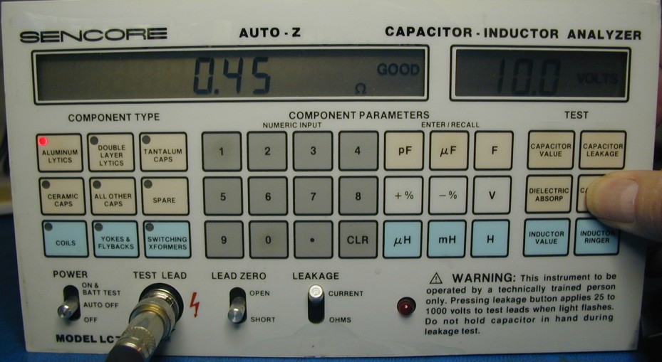
I recently watched a series of videos on youtube covering the repair of a Sencore LC102. This is a piece of test equipment that I have been interested in for several years, so I decided to spend some time reverse-engineering the firmware and studying the schematics. I ended up buying an LC77, which is nearly identical to the LC102, just to have a unit here for reference.
The 80C39 MCU used in these models has an addressable code size of 2K bytes. But the MCU designers added a mechanism to allow jumping to code in a second bank of 2K and back. So a total of 4K of code can be used. The LC102 has 16K of code! This is accomplished by connecting two upper address lines of the code EPROM to port bits of the MCU. This creates four banks of 4K, each having two 2K banks that the MCU can jump between. When the upper address bits are changed, the MCU instantly switches to the exact same address in a different 4K block of the EPROM, so there must be a "landing spot" for it at that location. So there are actually 8 banks of code in the EPROM which all have addresses from 0 to 2K. The firmware jumps between 4K banks often and between 2K sections of the 4K banks even more often. This makes the code very difficult to follow, as it is constantly jumping around. In addition, code for some often-used functions is duplicated and the same code is in multiple banks, presumably to make it more accessible when needed. Examples of duplicated code are the routines that form the display data and send it out, and the code that reads the ADC data.
Since there are eight banks of code which all have the same addresses from 0-2K, I divided the 16K of the V17 EPROM that contains the code into eight files. Each file was submitted to the disassembler, then cleaned up and re-formatted so that it was acceptable as input to the TASM32 assembler. The binary file created by the assembler matches the same section of the original EPROM exactly. Banks are numbered 0-7, corresponding to the upper three address bit values that select them. File names indicate which bank they contain. Bank 6 is selected when the 80C39 boots, so the MCU jumps to address 0 in that file. Bank 6 also contains the code for scanning the front panel switches and jumping to the code that implements the various tests. I have added some information about CPU register usage at the top of the bank 6 file. I also added some information about what code is located in the different banks. You can find my disassembly files, along with some information about the switch matrix and LCD segment mapping, in an archive linked below.
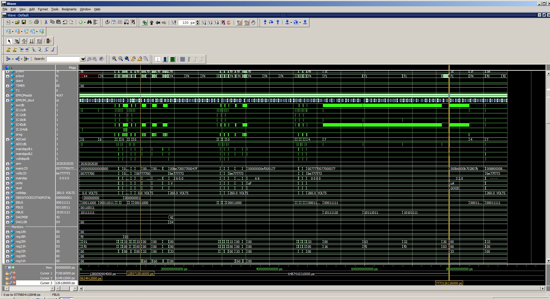
To get a better understanding of the firmware, I created a simplified digital simulation of the LC102/LC77. The simulation implements the switches and display, the MCU and its firmware, and the E, F, and H hw control registers. There is also a model of the ADC, with different output values depending on the test conditions. Using this model I was able to simulate an ESR measurement, and also a capacitor leakage measurement and see the correct results on the display, along with Good/Bad indication. I did not try to get the capacitor value, DIAB, or inductor tests working. To get the simulation working, I had to make some changes to the schematic. By this I mean that the service manual schematics for the LC102 did not work with the V17 firmware. The display chip decoding was not correct, and the switch positions in the matrix were also different. This caused a lot of frustration as I spent many hours trying to find my mistake when things didn't work. Once I realized that the schematic just didn't match the firmware, I fixed the display quickly. The switches were still not jumping to code that made sense. So I used my DMM to map out the switches on the LC77, and found that it matched the LC102 V17 firmware perfectly. Either the switch matrix was changed at some point, or it was simply drawn incorrectly. Below is a screen shot of the capacitor leakage simulation waveforms. You can see the main display and volts display, along with the qual (Good/Bad) and units icons. You can see the DAC value getting set when I entered the 260 volt value. The DAC value is always 65 times the voltage, so in this canse that would be 16,900 which is equal to 4204 in hex. This scale factor makes sense, since the maximum DAC value is 0xFFFF, or 65,535 in decimal, and the maximum voltage is 1000. You can see that during the capacitor leakage measurement, the swrdb signal is going low over and over. This is because the code is checking to see if the leakage switch is still pressed. I think you are required to hold it down during the entire test to see the result. We can't see the Leakage switch state here, but when I released the switch, the display was cleared.
In order to get the simulation working, I needed to figure out the mapping between the 96 LCD driver chip outputs and the segments and icons on the LCD. I also figured out the locations of each switch in the matrix in the LC77, which I think is the same as some LC102 units and perhaps all of them. Here is an archive containing that information along with the eight files containing the disassembly of the V17 code, with my comments.
Fuseholder fun:
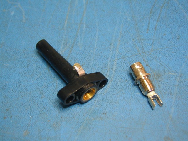
I wanted to insure that the installed fuse was the correct type, but when I tried to unscrew the BNC connector, it wouldn't budge. Tried even harder with just my fingers but no movement. So I put a pair of pliers on the round base of the connector and tried again. Of course the pliers slipped off, removing small bits of metal and marring the surface. The connector did not move. I didn't want to risk doing any more damage to the connector so I put a BNC T on the connector and put pliers on that to turn it. This was a really bad idea, as the two small posts that lock the BNC in place are not very strong, and I damaged one of them when I tried to unscrew the connector using the installed BNC T. This was not going well. So I removed the front panel and detached the fuse holder from it. By putting it in a vise, and using vise grips on the BNC base, I was finally able to unscrew the BNC, but it was still damaged from my initital efforts. I searched for "BNC fuse holder" but of course there is no such thing. Then I examined the parts and realised that Sencore had simply soldered a fuse clip onto a standard BNC jack to make it. Possibly they used silver solder. I ordered an Amphenol 031-2221 BNC connector from Mouser, unsoldered the damaged connector and installed the new one. I re-used the old solder, thinking it might be silver solder. The new BNC is pretty much identical to the original one. Then I soldered the red wire to the brass terminal, as it had come uncrimped previously. All fixed.
Please note: I have no connection to Sencore and never worked there. The information presented here is my own theory of how these units work and may contain errors. I will not be responsible for any damage to any unit caused by either proper or improper use of the information presented here.